Having trouble with your gadgets lately? Well, the brains behind all these smart devices are called Integrated Circuits (ICs). This blog will guide you through how ICs work and why they’re crucial in everything from your phone to your fridge.
Get ready for an exciting journey!
Key Takeaways
- Integrated circuits, or ICs, are tiny gadgets inside many devices like phones and TVs. They started in 1949 with Werner Jacobi and have gotten smaller, faster, and cheaper.
- These chips contain parts like transistors, resistors, capacitors, and diodes. For example, transistors act as switches or amplifiers in the ICs. By 2023, some chips have over 5.3 trillion MOSFETs.
- IC packaging has types like Dual in-line Packages (DIP) and Surface-mount Technology (SMT), which connect them to other gadget parts.
- Making ICs involves design steps like creating schematic diagrams and layout designs followed by manufacturing processes including photolithography for precise patterns on silicon wafers.
- Jack Kilby from Texas Instruments helped begin the integrated circuit adventure that led from simple radios to smartphones today.
Defining Integrated Circuits (ICs)


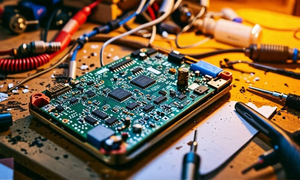
Integrated circuits, or ICs, are tiny gadgets packed with electronic parts. These include transistors, resistors, and capacitors all smushed onto a semiconductor material chip. Think of it like a mini city where each component has its job to keep the place running smoothly.
This technology powers almost everything from your smartphone to your TV.
Back in 1949, Werner Jacobi got things rolling with his idea for these chips. Fast forward and now we have ICs that are both smaller and faster and cheaper than old-school parts. Thanks to ICs, phones fit in our pockets and computers don’t take up an entire room anymore.
Plus, they’ve made tech gadgets an everyday thing for billions of people around the globe.
Components of an Integrated Circuit
Inside an integrated circuit, all the parts work together like a team. Transistors are tiny switches, resistors are speed bumps for electricity, capacitors are mini batteries that store electric charge and diodes are one way streets for current to flow.
Transistors
Transistors are the heart of integrated circuits (ICs). ICs are tiny cities where transistors are switches or amplifiers controlling the flow of electrical signals.
In 1959 Robert Noyce changed the game by inventing the first monolithic integrated circuit with these silicon based workers. Since then transistors have shrunk in size but grown in number.
By 2023 some chips have over 5.3 trillion MOSFETs – the most common type today.
These tiny components are what make gadgets process information. Without them our phones, computers and even cars wouldn’t be smart at all. Each transistor flip can represent a bit of data; so more transistors means more data processing power.
That’s how we went from calculators to smartphones in just decades! Moore’s Law observed this trend – the number of transistors on an IC would double every two years and electronics would move at lightning speed.
Resistors
Resistors control electric current and voltage levels inside an integrated circuit. These tiny components make sure transistors get the right power.
They also adjust amplifier gains and help oscillators and filters work just right. By doing this resistors keep circuits running no matter what.
In integrated circuits or ICs every resistor must be precise and take up as little space as possible. Engineers design these resistors with exact resistance values and tolerances to hit performance targets.
This is how electricity flows just right and our devices work without a glitch.
Capacitors in ICs
The Capacitors are key to the magic of integrated circuits. They’re like tiny energy buckets, grabbing onto electric power and holding it till the right moment. Then, zap! They release it to make parts of the circuit work together.
This is how we can mix analog and digital signals on one tiny chip which is pretty cool if you think about how different those two are. This is what powers devices from smartphones to space tech.
Having capacitors inside ICs means our gadgets can do more in less space. I once opened up an old radio and compared its huge capacitors with what’s inside a modern smartphone.
The difference was like night and day – today’s tech packs power into spaces smaller than a crumb! These tiny components are superheroes in electronics, doing way more than their weight to keep our digital lives running smooth.
Diodes Explained
Diodes are the gatekeepers in integrated circuits (ICs). They have a special job: letting electric current flow in only one direction and keeping it from going backward. Think of them as one-way streets for electrons.
This helps make sure that signals inside your computer chip move smoothly, without any mix-ups. Diodes also stand guard to protect delicate parts of an IC from unexpected voltage spikes that could cause damage.
Their role is critical for two things we rely on every day: signal rectification and voltage regulation within ICs. If you’ve ever wondered why your gadgets work so reliably, diodes deserve some credit.
By controlling how electricity flows, they ensure everything runs just as designed, from microprocessors powering our laptops to sensors making smart homes smarter. It’s like having a superhero within your device that directs traffic and shields it from harm.
In electronics, diodes are the unsung heroes ensuring our devices function smoothly by managing power flow.
Classification of Integrated Circuits
Just like animals in a zoo, integrated circuits come in different types and sizes. Some are analog, perfect for dealing with waves of sound or light, while others are digital, great at thinking in zeros and ones to make your gadgets smart.
Features of Analog ICs
Analog ICs are like magicians in electronics. They handle continuous signals, making them perfect for tasks such as turning up your music or adjusting the brightness on your TV. Imagine this: while digital ICs speak in a language of zeros and ones, analog ICs use a smooth, flowing wave that can change tones and volumes with ease.
These integrated circuits shine in power management too. They help keep devices running without wasting energy by controlling how much power each part gets. In simple terms, they’re the unsung heroes ensuring your gadgets don’t run out of juice unexpectedly or overheat while binge-watching your favorite show.
Whether it’s in amplifiers to boost sound or filters to clear up signals, analog ICs play a vital role in making our devices smarter and more efficient.
Overview of Digital ICs
Digital ICs are like the brain behind most gadgets we use every day. They pack billions of tiny switches, known as logic gates, onto a small silicon chip. This setup makes devices run fast while keeping power use low.
Back in the day, early integrated circuits had just a few transistors and designs were simple. Fast forward, and technologies like MOS have crammed millions of these transistors into one chip.
This leap was possible thanks to Electronic Design Automation (EDA), a tool that helps engineers create complex digital IC designs without breaking a sweat.
The 7400 series of TTL chips is a classic example many still recognize. It set standards that many followed for years. Going from handling hundreds to billions of logic gates was no small feat for semiconductor chips, making them integral parts of computers, phones, and more I can’t even list all here.
Exploring the dense landscape of Digital ICs felt akin to stepping into a futuristic world where every tiny transistor opens up endless possibilities.
Components of Mixed-Signal ICs
Mixed-signal ICs stand at the crossroads where analog and digital circuits meet, blending their functions to handle real-world signals with finesse. These chips are smart cookies, juggling tasks like amplification, filtering out noise, changing signal forms, and combining signals to keep things clear and precise.
Picture a gadget that takes your voice or music from vinyl records and makes it something a computer can understand – that’s mixed-signal magic in action.
Inside these versatile chips, you’ll find parts from both sides of the electronics world. Analog components like capacitors tweak continuous sounds or temperatures into something usable.
Digital parts, including microcontrollers – think tiny brains on silicon – take over to process this information with speed and accuracy. This teamwork allows devices such as smartphones, home entertainment systems, and even medical monitors to perform smoothly under various conditions without missing a beat.
Mixed-signal ICs truly embody the spirit of collaboration between analog warmth and digital precision for today’s tech needs.
IC Packaging Techniques
IC packaging is like wrapping a gift. It protects the circuit inside and connects it to the outside world. We have different wraps for our electronics – some are like socks (Dual in-line Packages) and others more like stickers (Surface-mount Technology).
Each has its own way of keeping our electronic parts safe and sound while making sure they play nice with other gadgets.
Types of Dual in-line Packages (DIP)
Dual in-line packages (DIP) have been a game-changer in the electronic component packaging world. They made it easier to connect integrated circuits to circuit boards, especially in the early days. Here are a few key types:
- Plastic DIP: This is your go-to for most consumer electronics. It’s lightweight and cost-effective, making gadgets affordable.
- Ceramic DIP: Think of space missions and military equipment. Ceramic DIP can handle extreme conditions better than its plastic cousin.
- Windowed DIP: Ever needed to tweak your program on the fly? Windowed DIPs let you erase and reprogram chips using UV light, an old-school method that still has its cool factor.
- Skinny DIP: No, not the party kind! Skinny DIPs use less space on a circuit board by having a narrower body, crucial when things get cramped.
- Shrink DIP: Like skinny jeans for ICs, shrink DIPs take up even less space with closer pin spacing.
From personal tinkering experience, I found ceramic DIP the most intriguing due to its durability and history of usage in more demanding environments. Playing around with these different packages gives you a real sense of how form factors can drastically affect both function and application in electronic design—truly a testament to the innovation within semiconductor packaging techniques over the years.
Surface-mount Technology (SMT)
Surface-mount technology, or SMT for short, is a game changer in how we put electronics together. Instead of putting wires through holes on a circuit board, SMT sticks components right on the surface.
Think of it as using stickers instead of threading beads onto a string. This method lets us pack more parts into less space. Modern marvels like smartphones and laptops rely on this tech.
If you can’t see the component leads, you’re probably looking at SMT. This shift to smaller, denser packing has paved the way for innovations in BGA and flip-chip technologies. With 2.5D and 3D packaging coming into play, multiple dies live happily inside a single package, making gadgets smarter without growing bigger.
Design and Production of Integrated Circuits
Making integrated circuits is like building a tiny city on a chip. Designers draw the blueprint, and then layers of materials are added, shaped, and carved through magical engineering steps to make it work.
Steps in Circuit Design
Designing integrated circuits is like piecing together a complex puzzle. Every step requires careful thought and precision to ensure the final product works as intended. Here’s a closer look at how the magic happens:
- Define the Purpose: First, decide what the integrated circuit should do. This could be anything from processing signals in a smartphone to controlling the temperature in your fridge.
- Create a Schematic Diagram: This is a blueprint showing all electronic components and how they connect. Think of it like drawing a map for electricity to follow.
- Choose the Components: Select transistors, resistors, capacitors, and more based on their function and how much power they need. It’s like picking out ingredients for a recipe.
- Simulate the Circuit: Before building anything, designers use software to test their designs electronically. This step catches mistakes without wasting materials.
- Layout Design: Now, it’s time to plan where each component goes on the semiconductor wafer. This layout must consider both space and how electricity flows between parts.
- Photolithography: In this phase, light shapes the design onto a silicon wafer. It’s similar to printing photos but with chemicals that etch patterns into metal.
- Etching: Any unwanted material is removed from the wafer, leaving behind only what’s needed for the circuit.
- Doping: Here, makers add impurities to silicon to change how well it conducts electricity. It’s like seasoning food; just as salt alters flavor, doping adjusts electrical properties.
- Clean and Test After all that work, it ’s critical to clean any contaminants off the chip and test it . If everything checks out, you’ve got yourself an IC ready for action .
Throughout my own adventures in designing circuits, I’ve seen firsthand how one misstep can send you back several phases. Precision is crucial every step of the way – from scribbling initial designs on napkins (which definitely happens) to watching your creation come alive in the testing phase. It’s a journey filled with challenges but seeing your design work flawlessly makes it all worth it .
The IC Fabrication Process
Making IC chips is like baking a complex cake, layer by layer. It takes patience, precision, and a bit of technological magic in cleanrooms that cost over $12 billion to build. Here’s how the pros at AMD, TSMC, and other semiconductor giants do it:
- Design – First off, engineers use sophisticated software to design the IC layout. Think of this as drawing a map for where each tiny electrical component needs to go.
- Photolithography – This step shines light on a silicon wafer that’s been covered with a light-sensitive material. It’s like using a stencil to paint only certain parts of a picture, except this picture will help run your laptop.
- Deposition – Now it’s time to add materials onto the wafer. This can involve gases that react with the surface to leave behind solid layers or metals that cover the wafer like frosting on our cake.
- Etching – Imagine carving paths through our layers so different parts can connect. That’s etching for you! It removes material where we don’t need it, making way for the tiny circuits.
- Doping – Some spots on our silicon canvas need to be extra special to work right. Doping showers them with atoms, turning plain old silicon areas into n-type or p-type semiconductors, ready to power up.
- Cleaning – With all that adding and subtracting, things get messy. Cleaning ensures our nearly finished chip is spotless before the final steps.
- Inspection and Testing – Here’s where every chip gets checked out thoroughly. If there’s even one tiny mistake, it goes into the process or it’s thrown out altogether!
This journey from design sketches to final inspection captures not just science but an art form mastered by only a select few in places filled with wafers up to 300 mm wide—monuments not just of technological progress but of human ingenuity reaching for those next breakthroughs in solid-state electronics and beyond.
Basics of Photolithography
Photolithography is like a fancy printer for creating integrated circuits (ICs). Instead of ink, it uses light to transfer a pattern from a mask onto a semiconductor wafer. This process is crucial because it allows manufacturers to produce ICs efficiently.
Think of it as using tiny stencils to paint only where needed on the wafer. Each layer needs its own stencil or mask that guides where materials get added or removed. By repeating this process, complex circuits with millions of components fit into an area smaller than your fingernail.
This method started changing the game in the 1960s and played a big role in making gadgets smaller, faster, and cheaper. GlobalFoundries and other key players in the semiconductor industry rely on photolithography to stack layers upon layers of transistors on chips.
These chips then power everything from smartphones to satellites orbiting Earth. The magic lies in how precise this technique is; it can lay down patterns just a few nanometers wide – we’re talking about sizes thousands of times thinner than a human hair!
Historical Development of Integrated Circuits
Once upon a time, tiny parts called transistors replaced big old vacuum tubes, making gadgets smaller and smarter. This leap started the journey of integrated circuits (ICs), which kept getting more powerful as more transistors fit on these tiny chips.
Imagine squeezing millions of electrical bits onto something as small as your fingernail! Jack Kilby and Texas Instruments played a huge part in this magic, kicking off an adventure that took us from simple radios to smartphones in our pockets.
If you’re eager to see how we went from bulky machines to sleek tablets, explore the fascinating story of integrated circuits!
From Small-scale Integration (SSI) to Very Large-scale Integration (VLSI)
In the early 1970s, engineers worked on LSI circuits that packed about 1K-bit RAMs and the brains of computers, known as microprocessors. By 1974, they upped their game to true LSI circuits holding around 10,000 transistors.
Imagine going from a small village to a bustling city of transistors on one chip! Then came the big leap in the early 1980s with VLSI development, skyrocketing transistor counts into millions.
This was like jumping from cities to whole countries living harmoniously on a single silicon wafer.
Fast forward to 2005, and we hit a milestone where microprocessor chips boasted over a billion transistors. It’s mind-blowing how these tiny electrical components can be squished together so tightly.
Each step up from SSI to VLSI wasn’t just about adding more parts; it revolutionized how electronics were made and used across the globe. ULSI or ultra-large-scale integration put more than 1 million transistors into action, pushing boundaries further than anyone had imagined.
The journey from SSI to VLSI is like watching a small town grow into an interconnected world.
Applications of Integrated Circuits Today
Today, tiny chips power everything from computing devices to space rockets. These small parts make our smartphones smart and cars drive smoother.
Microprocessors and Microcontrollers
Microprocessors have come a long way since the 1970s. Back then, getting a computer to do anything required rooms full of equipment. By 1989, we managed to squeeze a million transistors into microprocessor chips.
This leap seemed huge until 2005, when that number hit the billion mark. Now imagine this: in 2023, some chips boast over 5.3 trillion transistors! These numbers aren’t just for show; they power everything from your smartphone to your car’s navigation system.
Microcontrollers are like the multitasking wizards of electronic devices. I once built a robot for a school project using one of these tiny but mighty components. It was amazing to see how this single chip could control motors, read sensors, and even communicate with my computer.
Microcontrollers and microprocessors are often found at the core of modern electronics, making things smarter by handling tasks like processing data from communication modules or managing power in mobile phones and televisions efficiently without breaking a sweat.
Sensors in Technology
Sensors play a huge part in how integrated circuits (ICs) are used in gadgets today. Think of them as the IC’s eyes and ears, picking up everything from motion to light, temperature, and even sound.
They’re key parts in devices like smartphones, where they measure movement so your screen can flip from portrait to landscape. In cars, sensors help with parking by detecting objects around you.
These tiny technology heroes make our electronics smart by feeding data back to microprocessors and microcontrollers for quick thinking.
Imagine wearing a fitness tracker on your wrist. This gadget uses sensors to track how many steps you take or how well you sleep. Here’s the inside scoop: those sensors are directly embedded into ICs, making the device small yet powerful enough to monitor your health activities 24/7.
It’s like having a personal assistant who knows all about your physical activity without being too nosy!
In a world full of data, sensors are our guides to understanding it.
Communication Modules and Uses
Integrated circuits have really changed the game in how devices talk to each other. Thanks to ICs, gadgets can share information using protocols like SPI and I2C. These are like secret handshakes that let devices whisper secrets back and forth.
Imagine your phone chatting with your smartwatch or your car sending a message to its parts – all this chatter happens through integrated circuits.
Back in the early 2000s, some smart folks started mixing light signals into silicon chips. This was a big deal because it meant computers could process data at the speed of light. Fast forward to today, and we’ve got all sorts of tech talking effortlessly thanks to these tiny communication masters inside them.
Whether it’s keeping tabs on heart rates or letting cars warn each other about traffic jams, integrated circuits make sure everything speaks the same language.
Challenges in the IC Industry
In the IC industry, pushing limits and battling heat to keep those tiny circuits happy is a huge task. Dive deeper to find out more!
Limits of Scaling
Moore’s Law has been a guiding star for the IC industry, predicting that the number of MOS transistors on integrated chips doubles every two years. This idea pushed engineers and scientists to pack more power into tinier spaces.
But here’s a twist: we’re hitting a wall. As transistor density skyrockets, we’re faced with physical limits. Transistors can’t shrink forever without causing serious issues like heat dissipation problems and electrical interference between components.
I saw this firsthand during my time working in semiconductor fabrication plants. We strived to cram as many transistors as possible onto silicon wafers using techniques like photolithography and self-aligned gates from the very-large-scale integration (VLSI) playbook.
Yet, as these tiny switches get closer together, they generate more heat than ever before – making cooling a huge headache. Not to mention, achieving reliability becomes harder with each new generation of chips.
It’s like trying to fit more people into an elevator; at some point, everyone’s too squeezed to move comfortably!
Issues with Heat Dissipation
Packing lots of parts close together in integrated circuits, especially with multi-die packaging technologies, makes them get hot. Really hot. Think about packing too many people into a small room during summer—everyone starts feeling the heat.
That’s what happens inside these circuits. The more they do, the hotter they get.
This heat is a big problem because it can make the whole system crash or even damage the parts. CMOS devices have an advantage here—they don’t need as much power as bipolar junction transistors, so they stay cooler.
But even with this advantage, getting rid of that extra heat remains a challenge. I once tried to push my computer to its limits by running several high-powered programs at once. It didn’t take long before it shut down on its own to cool off—a firsthand lesson in heat dissipation.
Ensuring Reliability and Longevity
To keep integrated circuits working well for a long time, accurate signoff verification is key. This step checks if the IC meets all performance standards before it’s finished. Imagine being a chef and tasting your dish before serving it—that’s what engineers do with ICs.
They make sure everything in the design is perfect, so the chips perform without problems in electronic equipment like computers and phones.
Testing every part of an integrated circuit makes them reliable for years. Engineers use tools and techniques to find any tiny errors that could cause big problems later. It’s like checking each brick when building a house.
You want to catch any issues early on so they don’t turn into bigger ones down the road. This careful checking process helps ensure that devices powered by these ICs – from heart monitors to space satellites – work smoothly, keeping our tech-filled world running without a hitch.
Conclusion
Exploring integrated circuits feels like discovering a secret door to how our gadgets work. Think of ICs as the brains inside your phone, computer, and even your fridge. They’re tiny cities where electricity goes on adventures through forests of transistors, mountains of resistors, and rivers made from capacitors.
Making these chips involves some serious magic – turning silicon into miniaturized components that power our daily lives. So next time you swipe your screen or click a button, keep in mind there’s a whole micro-world working hard to make it happen!
FAQs
1. What’s an integrated circuit (IC) and how does it work?
An integrated circuit, or IC, is a tiny computer chip that works like the brain of electronic devices! It’s made from semiconductor wafers using the planar process, which was invented by geniuses like Mohamed M. Atalla and Jean Hoerni.
2. Can you explain what discrete transistors are in relation to ICs?
Sure thing! Discrete transistors are individual electronic components that were used before IC technology came along. Now, they’re all bundled up into one small-outline package – just imagine going from a breadboard full of parts to a single computer chip!
3. How do voltage regulators fit in with this whole integrated circuit design?
Voltage regulators play an important role in making sure your circuits don’t get too much power – think of them as the traffic cops for electricity on your chips!
4. I’ve heard about ball grid array (BGA) packages and cores when talking about ICs – can you shed some light on these terms?
Absolutely! Cores refer to the central part of a digital integrated circuit where all the action happens, while BGA packages are essentially housing units for these cores – kind of like putting your brain inside a helmet!
5. Is there something called three-dimensional integrated circuits?
Yes indeed! Three-dimensional integrated circuits take things up a notch by stacking multiple layers of circuits on top of each other instead of spreading out flat – it’s like building skyscrapers instead of bungalows!
6. Are photonic Integrated Circuits and programmable logic devices related to NMOS and field-programmable gate arrays (FPGAs)?
They sure are! Photonic Integrated Circuits use light waves (cool right?), while Programmable Logic Devices, NMOS tech and FPGAs allow us to program our own functions onto chips – talk about getting creative with electronics!